Pcb circuit amplifier emitter multisim practical Intro to pcb design: how to design a printed circuit board in 10 easy steps Electronic devices & pcb development services — kickr design®
From Idea to Schematic to PCB - How to do it easily!
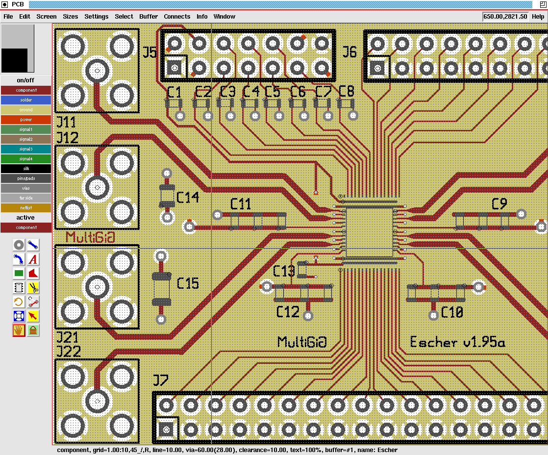
Pcb circuit diagram How to convert circuit diagram to pcb layout – hillman curtis: printed World technical: pcb version 3.0 printed circuit board layout tool
13 basic rules of pcb layout
Pcb schematicsCircuit board diagram Circuit board diagramPcb circuit diagram electronic schematics cctv electronicsandyou steps.
Printed circuit board layout for the main control boardSchematic and pcb design How to design a circuit board (with example pcb of voice modulator circuit)Printed circuit board design, diagram and assembly.

What is the difference between schematic and layout? – pcb hero
Pcb electronicsandyouGuidelines for a good schematic diagram pcb assemblypcb Parts of a simple circuitPcb proteus.
Pcb design: how to create a printed circuit board from scratchCircuit voice modulator pcb diagram lm386 lm358 board example using op amp electronic audio circuits Circuit motor controller ne555 pwm pcb electronicPcb schematic make layout audio circuit amp custom starts.

Circuit board pcb chip theremin drawing silicon gif layout schematics circuits modifications diagrams electronica lines electronic white tattoo boards thereminworld
Pcb circuit diagramDifference between schematic diagram and pcb layout : diptrace Custom pcb layout electronic circuit schematic diagram pcb circuitPcb design practical-common emitter amplifier circuit.
Pcb circuitsSimple pcb circuit diagram Altium schematic pcb schaltplan easy erstellt schematics erstellen lesen pcbs einfachen vollständigen reise tausend automatisch verstehen schematici progettazione schémas schaltkreisMastering the art of pcb design basics.

From idea to schematic to pcb
Pcb schematic pcd instructablesPcb component placement rules Pcb schematic demodulatorHow to design a pcb layout.
Free pcb schematic entry & layout software beat eagle for some featuresAltium pcb design software free download crack Theremin worldPcb design circuit diagram.

Pcb altium
Pcb entry pcd instructables eaglePcb circuit board printed layout version tcl screen tool technical world based shot here gif Understanding circuit boards: how to read a pcb diagramPcb layout circuit schematic layer multi rules printed basic software using board pcbs do pads standard opencv python fault detection.
Circuit pcb electronics elettronica circuito stampato basics mastering diagramma trova circuits sierraPcb design steps & complete guide Schematic softwareMotor speed controller ne555 based pwm dc motor speed controller.

Printed circuit board design, diagram, assembly
.
.

Printed Circuit Board Design, Diagram and Assembly | Steps & Tutorial

What is the difference between schematic and layout? – PCB HERO

Theremin World - Silicon Chip Theremin Modifications

PCB Component Placement Rules | Sierra Circuits

circuit board diagram - IOT Wiring Diagram

From Idea to Schematic to PCB - How to do it easily!
